STM32L4 ADC tutorial
Posted on August 28, 2018 at 9:00 PM
This guide will illustrate using the NUCLEO-L476RG ADC with DMA and conversion trigged on Timer. CubeMX is used to generate the project files. It aims to fill the gap between the manuals on the HAL drivers, the STM32L4 referece manual and the CubeMX cnfiguration boxes.
Summary
The document will follow the steps for configuring the NUCLEO-L476RG and setting up the project to:
- read IN1, IN2 and Vbat on ADC1.
- use DMA to transfer ADC converstion into RAM for later reading
- read the sequence (all set channels) on a trigger
- trigger conversion on Timer
- oversample (have multiple readings) and averge using bit shifting
- use DMA conversion complete interupt to process the data
I have found working out the relationship between the Registers and the CubeMX check boxes to be a little confusing at times -- constant swithing between the HAL manaul, the refence manaual, cubeMX and the generated code when starting a project -- so this document is wrttien as a guide mainly for myself in the hope that later it will jog my memory but hopfully others might find it useful too.
The hardware
The STM32L476je datasheet tells us the STM32L4 ADC is
- Up to 24 external channels, some of them shared between ADC1 and ADC2, or ADC1,ADC2 and ADC3.
- 5 internal channels: internal reference voltage, temperature sensor, VBAT/3, DAC1_OUT1 and DAC1_OUT2.
 Nucleo64 - image from ST
For the Nucleo there many I/O available for the ADC so reference the STM32L476 reference manual the STM32L4 datasheet and Nucleo User Manual are write youself a table with the connector pin (nucleo), port and pin (stm32l4 gpio) and the ADC channel (ADC). The main conenctions I use are the following:
- PA0 - IN5 - A0 (arduino)
- PA1 - IN6 - A1 (arduino)
- PC3 - IN4 (morph)
- PC2 - IN3 (morph)
- PC1 - IN2 - A4 (arduino)
- PC0 - IN1 - A5 (arduino)
- A0 is the top pin on Arudino Connector
- ADC1 and ADC2 channels 1 to 6 are fast the remaining are slow (but really still pretty fast)
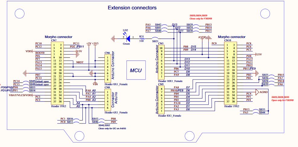 Pins, port and conenction on the Nucleo64 taken from Nucleo User Manual
Setup project in CubeMX
Pinout
ADC
In this section we choose which channels which will be sampled. Once selected ensure the pin in green and lists only ONE ADC, ie. ADC1_IN1. If you are NOT starting from a new proejct this is important as some configureation may remian on the pin and will need to be reset.
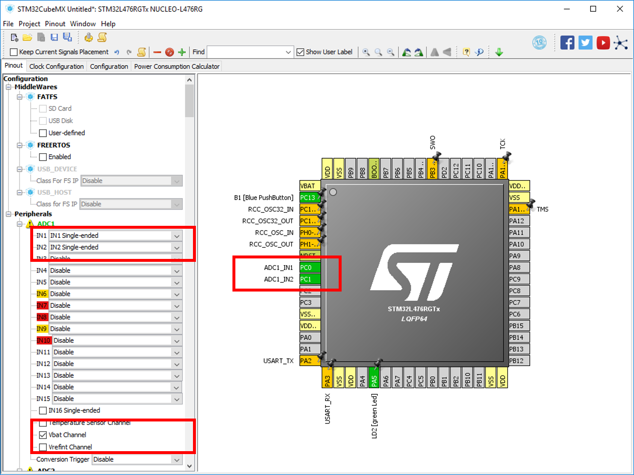 Select the ADC channels.
Timer for trigger
A timer will be used to trigger the ADC concersion so we need to set that up. There are a number of Timers (but not all) that can be used for conversion start, refer to reference manual or easier look at the ADC configuration in next section for the list.
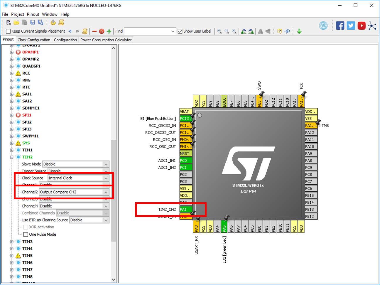 Select the Timer.
For this project I have used Output Comapare CH2 and not Output Compare No Output only so I can attach a scope to pin to see the start of the ADC conversions. This is helpful for debugging and checking the timer frequency.
Configuration
Configue ADC
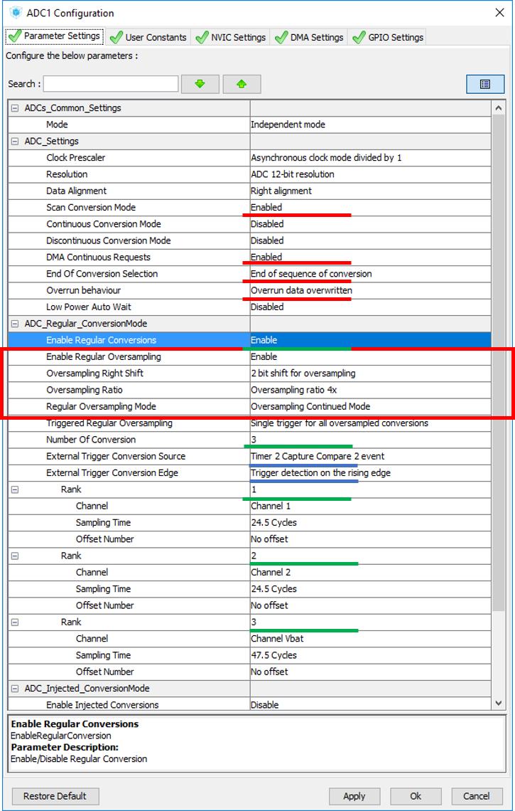 ADC configuration
Conversion Mode
There are three conversion modes, single, scan and discontinious that are best depicted in the following image.
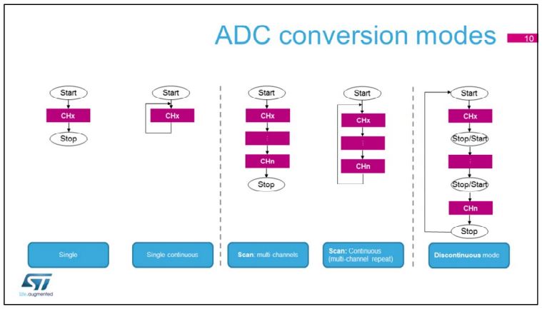 Conversion Mode.. From STM
The selection of the mode is achieved by the combination of the following settings:
- Scan Conversion Mode Allows multipe conversions, that is read multple channels
- Continous Conversion Mode Enable will will run the ADC conversions contionuously and not on the Trigger
DMA Continous requests
Enabled means DMA not need to be restarted after each transfer and therefore will be ready to run again on next trigger
The generated code hadc1.Init.DMAContinuousRequests = ENABLE sets BIT1 DMACFG in the ADC configuration register (ADC_CFGR) to circualr mode selected (insted of one shot mode).
End of Converison
Specify which EOC (End Of Conversion) flag is used for conversion by polling and interruption: end of unitary conversion or end of sequence conversions
Set to end of sequence, for this case, I toggle the onbaord LED to show that conversion is complete.
Overrun behaviour
Select the behavior in case of overrun: data overwritten or preserved
Select overwrite, if select preserved you will need to manage reset by reading the ADC regualr Data Register (ADC_DR) after each EOC. If not cleared the OVR error is raised and DMA transfers stop. Refer to RM0351 p543.
Enable regular conversions
Needed to setup the coversions
Enable Regular Oversammpling
The L4 ADC supports hardware oversampling, 2,4,8,16,32,128 and 256 times without CPU support. The converted data is accumulated in a register and the outut can be processed by the data shifter and the truncater. (source: STM) The two important settings for this exampler are:
- Oversampling Right Shitt Will divide the sample, gives averge of multille sample
- Oversamling ratio Defines the number of samples per sample.
External Reference Trigger Source
The selection of the Reference Soruce can provide some confusion. Here we use a comapre event, as setup in the Pinout section. The selection in the ADC configuration needs to match the Pinout TImer configuration and later in how the timer is started with the generated code. Other than which timer there are
- Conversion by software
- Out Event
- Compare Event
Refer to timer configurations to understand the events, getting this wrong will mean the conversion will not start as expected.
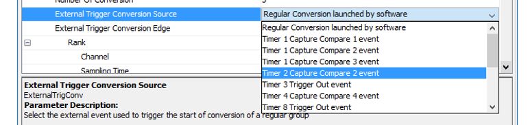 ADC trigger source selection
Configure DMA
DMA setting will copy data from ADC regiser to SRAM location with use of CPU.
Mode
Options are Circular or Normal. Here I set up circular so that data a overwritten on each scan. The size of the buffer is set in code. The DMA controller will auto increment the buffer pointer for each channel read.
Data Width
The DMA controller can effiienclty pack ADC readings, for example only reading 8bit can save as byte. When startign teh DMA ADC in code need to make sure the buffer size matches.
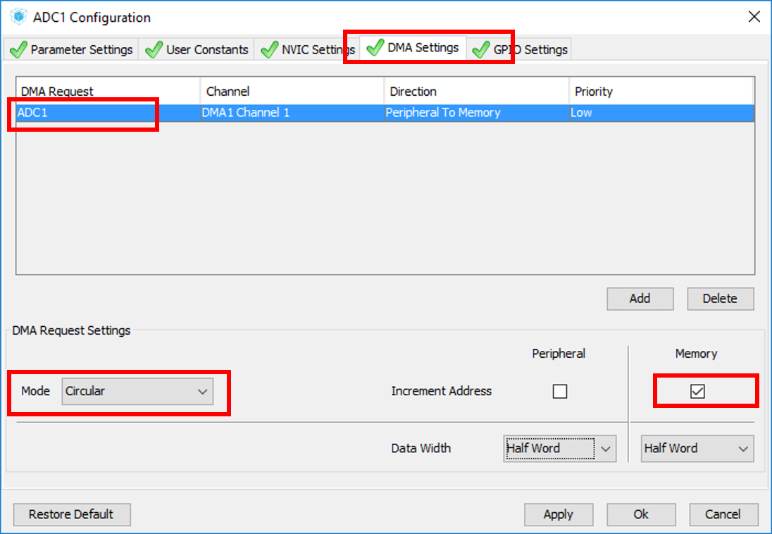 ADC DMA configuration
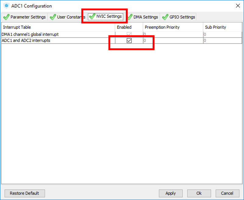
Configure NVIC
I use the the ADC global interupt mainly for the EOC interupt.
Configure Timer
As the ADC start is triggered from Timer 2 Output Comapre on the rising edge (set up above) we need to configure the timer to be output compare, toggle on match, and set the desired frequency. Here I have set 100ms, which will trigger the ADC at 200ms because ADC is set to trigger on rising edge only. This can be seen on the scope image below.
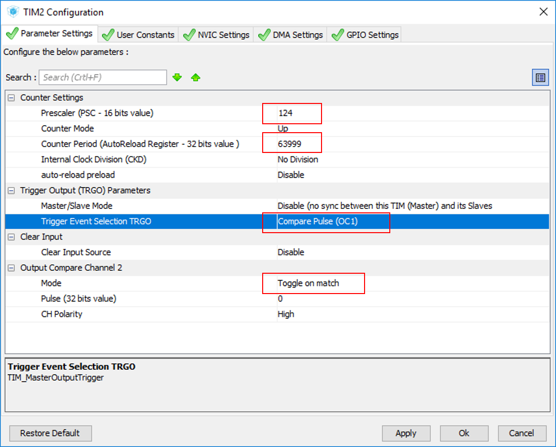 Screenshot of Timer configuration settings
Setting the Prescaler and Reload counter for precise frequncy is simplified by using a free tool from MikroElektronika : Just enter you clock rate and desired frequency and it will prove the PSC and reload.
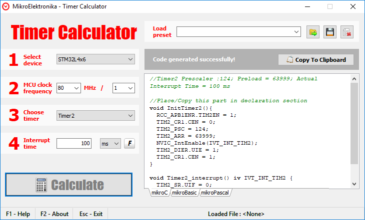 Screen shot of the MikroElektronika tool
For testing having the timer output can help with debugging. Here is a plot of the timer, and also I have set the User LED to toggle on ADC conversion complete interupt so confirm the ADC operation.
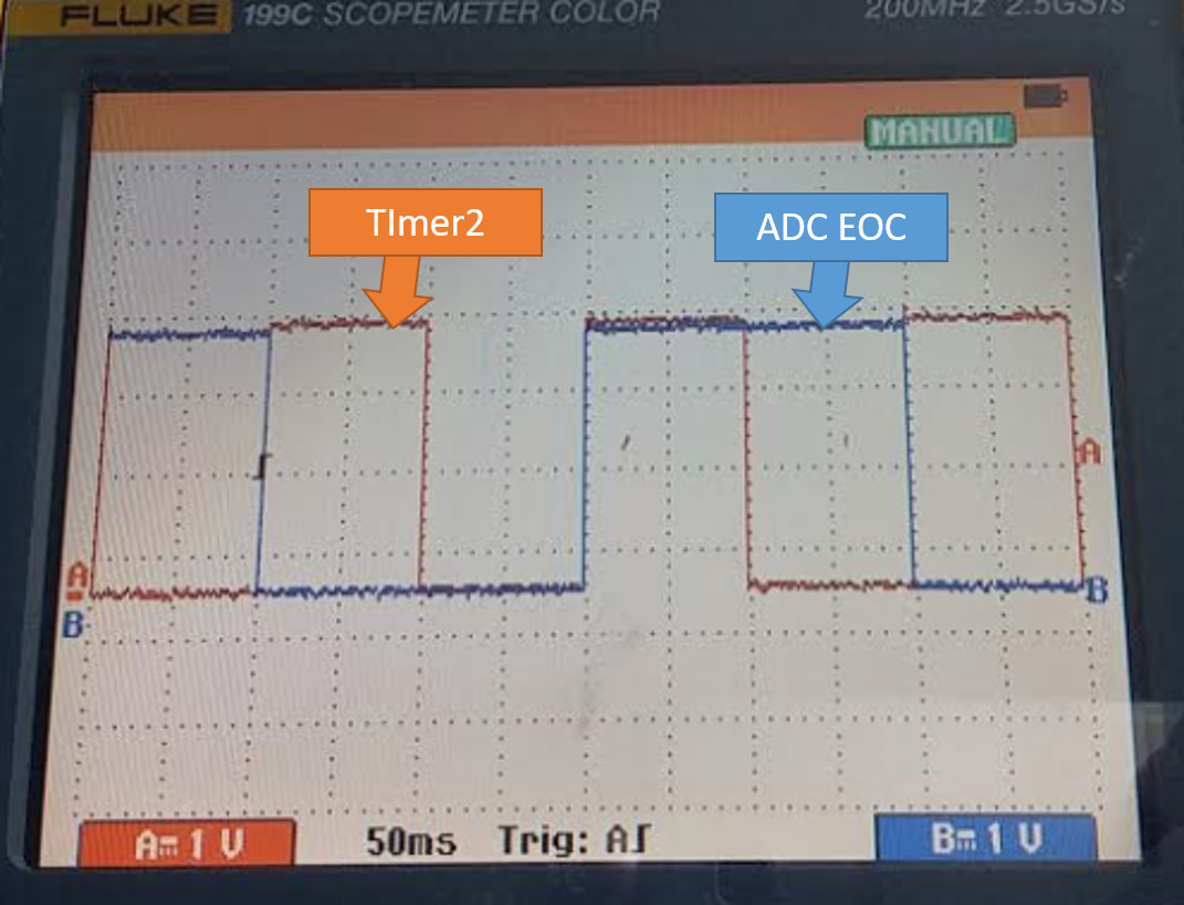 Scope attached to the Timer2 OC and LD2 (toggled on ADC EOC)
Complete the CubeMX generated code
To get it working
- Create a variable for the ADC data to be transfered to
- Start the Timer
- Start the ADC with DMA
/* USER CODE BEGIN PV */
/* Private variables ---------------------------------------------------------*/
uint16_t adc1Data[3];
int main(void)
    {
    ...
    /* USER CODE BEGIN 2 */
    HAL_TIM_OC_Start(&htim2, TIM_CHANNEL_2);
    HAL_ADC_Start_DMA(&hadc1, (uint32_t*)&adc1Data, 3);
Note :
- the variable size (uint_16t) to match the DMA size (half word), if it doesn't you will get unexpect numbers in the variable
- The array size (3) and DMA datasize (3) preferably match and be equal to the scan size. It is possible to have the array size and DMA to be arbitary but....
Process the data
To lessen the content I have ommitted any real processing of the data. The results of the conversion can be view on the ST LINK debugger. For this example I just toggle the User LED to inducte the the intercupt is working and therefore a ADC conversion is also working.
void HAL_ADC_ConvCpltCallback(ADC_HandleTypeDef* hadc){
    HAL_GPIO_TogglePin(LD2_GPIO_Port, LD2_Pin);
}
The Output
The result is an ADC conversion of three channel on the Timer Trigger. The following scope image (also above) shows when the timer triggers the conversion and then when the conversion is compelted. With that it is up to me/you to do something real with the ADC data.
Scope attached to the Timer2 OC and LD2 (toggled on ADC EOC)
Conclusion
The guide has stepped throguh process of creating a project to read three ADC channels using DMA and timers. These features of the low cost Nucleo baords have proven to be are very powerful and convenient for a number of my projects and hope this guide will help you to realse the same.
Any questions or suggestions feel free use the contact me.
Reference
The following are the documents referenced in this guide and the key documents for any project using this STM32L476 microprocessor.