STM32L4 Nucleo ADC Conversion on Casacde Timer with CubeMX
Posted on July 31, 2018 at 9:00 PM
This guide will illustrate using cascaded timers on the NUCLEO-L476RG, one in PWM mode and the second in One Pulse Mode. In addition the second will also trigger a ADC conversion. The article uses CubeMX and HAL drivers to complete a example in ST Timer Cookbook that uses direct register settings and extends this to using the TRGO of the second timer to trigger the ADC conversion start.
Summary
ST provides a lot of excellent information and examples using the STM32 chips, however using CubeMX and using the HAL drivers is not well covered in these examples so I write these mostly to remind myself how what I have done so I can do it again!
The document will follow the steps for configuring the NUCLEO-L476RG and setting up the project to:
- cascade timers to create periodic N-Pulse output
- TIM2 with a PWM signal
- TIM8 in one pulse mode (OPM)
- Trigger ADC1 using TIM8 TRGO2 the dedicated ADC Timer output
The following image show that targeted wavefrom.
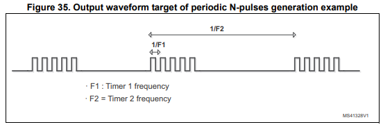 Output waveform Source: ST Timer Cookbook
The need for this waveform came from a proect that has a LED and photodiode, the LED is turned on and off on a timer with a fixed frequency and duty, say 50kHz and 60% duty and when the LED is on I want to measure the photodiode. But to get the sample accurate I then needed a deterministic delay to account for the capacaaance of the photo-diode amplifaciaiton and in addiotnal it turned out I also needed multiple pulses to calcualte the decay of the signal in the single pulse.
There are a number of alternative ways to do this with the STM32L4 ADC, is this document I will do it following the example in the Source ST Timer Cookbook but using CubeMX and HAL rather than direct register configuration.
The hardware
The STM32L476 datasheet tells us The STM32L476xx includes two advanced control timers, up to nine general-purpose timers, two basic timers, two low-power timers, two watchdog timers and a SysTick timer. Thats a lot of timers! For this project we use a General Timer(TIM2) and an Advanced Timer(TIM8). TIM2 will be used to generate the PWM output to drive the LED circuit and its Trigger Ouptut (TRGO) will trigger TIM8. TIM8 is used for two reasons, the main being it has a repition counter that will allow the generation of a N-pulse waveform, and secondly it has a dedicated Trigger Ouptut (TRGO2) for the ADC.
 Nucleo64 - image from STM
Setup project in CubeMX
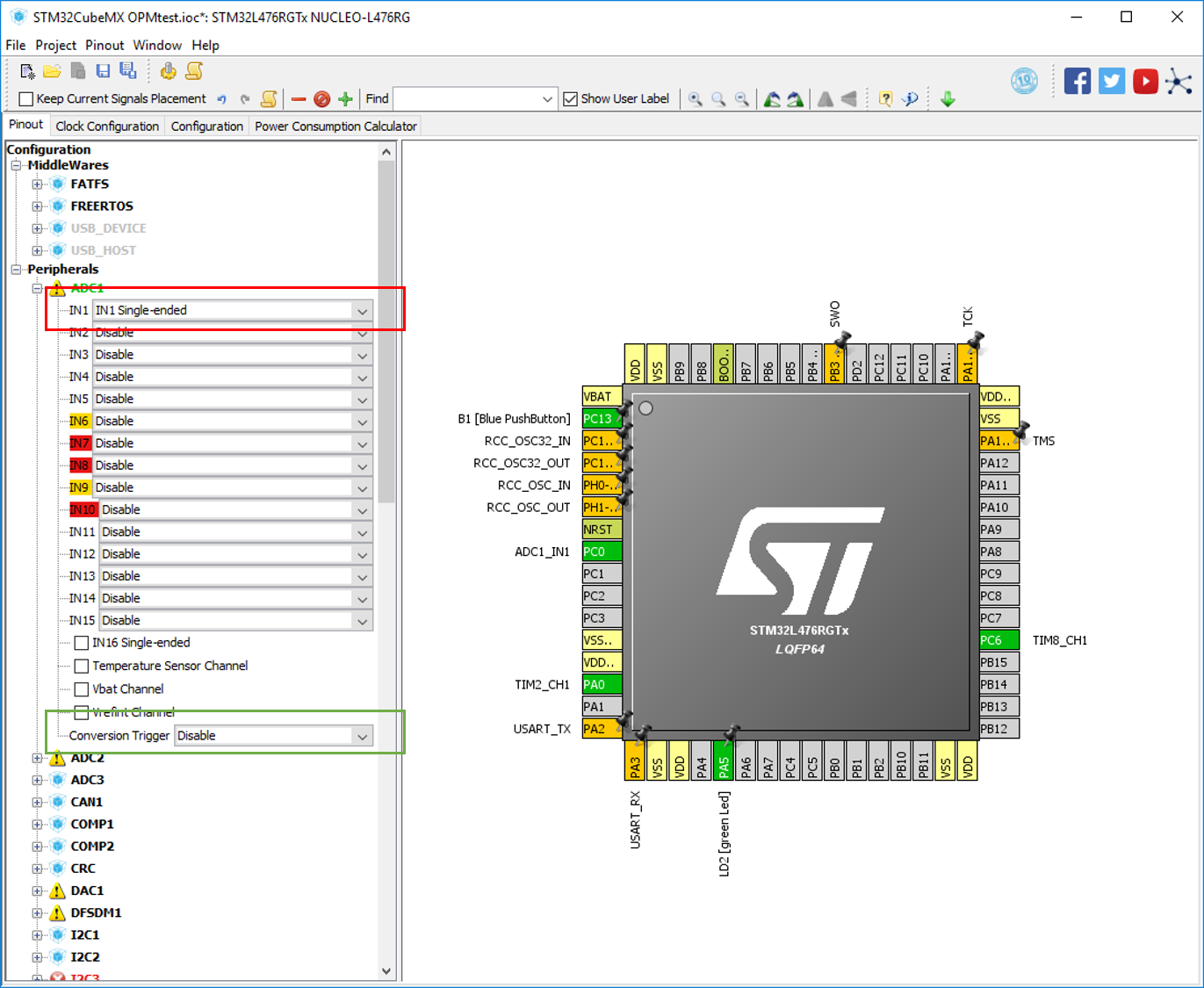
Pinout
The Timers
Trigger for ADC
The ADC have multiple options for triggers, these include Compare Event and TRGO output, and also TIM1 and TIM8 have a TRGO2 output dedicated to the ADC. Refer to the following table taken from RM051 Reference manual.
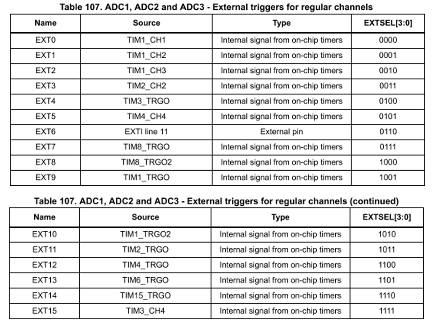 Possible ADC converstion triggers
Setup the Timer
For our case we choose Timer 2 for the LED PWM signal and Timer8 for ADC trigger.
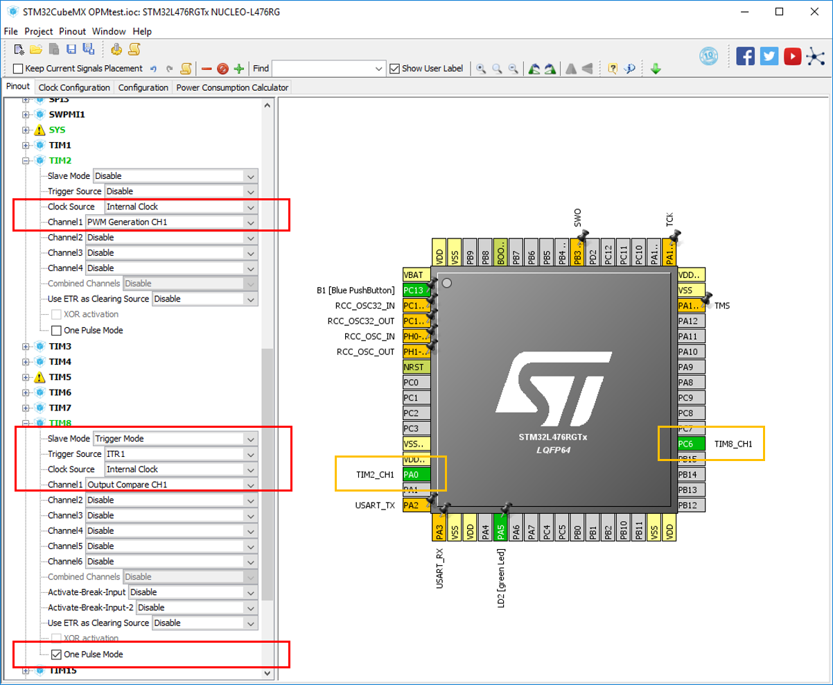 Timer setup
For this project I have used Output Comapare CH1 and not Output Compare No Output only so I can attach a scope to pin to see the start of the ADC conversions. This is helpful for debugging and checking the timer frequency.
There are two settings that are improtant for the function of cascade tiemrs, Slave Mode and Trigger Source.
Slave Mode is best explained by the follwoing slide from ST
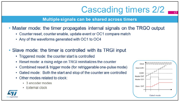 Slave mode settings. Source: ST Timer Cookbook
Trigger Source select what till trigger the starting of the timer counter. The following table from the Refence manual describes the internal connection possible. For our case the MAster is TIM2 so we wnat to use IT1
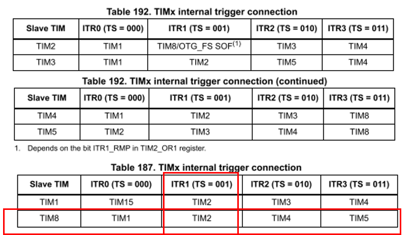 Internal Trigger
ADC
The focus of this guide is the Timers, so here we just select a single input for the ADC. Don't be fooled by the tick box for Conversion Trigger this refers to external trigger, a GPIO pin to use for the trigger.
 Select the ADC channels.
Configuration
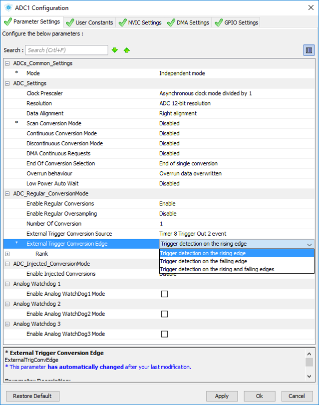
Configue ADC
Configure the ADC conversion. Main point for this simple conversion is External Trigger Conversion is set to TIM8_TRGO2 to match what I have configured in TIM8
 ADC configuration
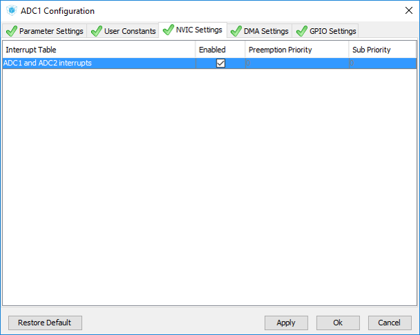
Configure NVIC
Enable the ADC interupt, we will use this to process the conversion result.
 ADC configuration
Configure Timer
Common for both timers is the setting the Prescaler and Reload counter. Setting the frequncy is simplified by using a free tool from MikroElektronika : Just enter you clock rate and desired frequency and it will prove the PSC and reload.
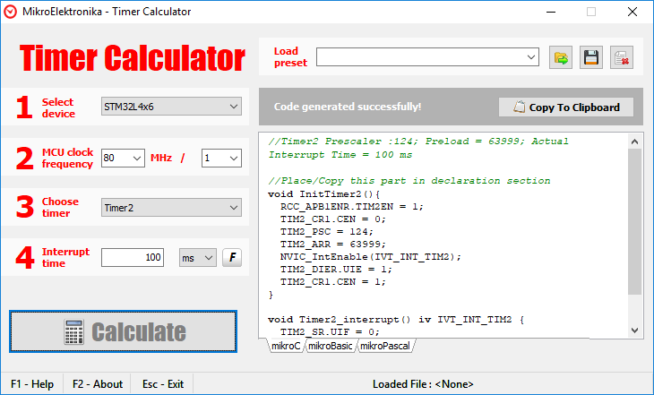 Screen shot of the MikroElektronika tool
TIM2 output will be used to drive the LED circuit and trigger TIM8. To drive the LED I setup the PWM Generation Channel with the the Mode and CH Polarity remembering
- PWM mode 1 = Set on compare match
- PWM mode 2 = Clear on compare match
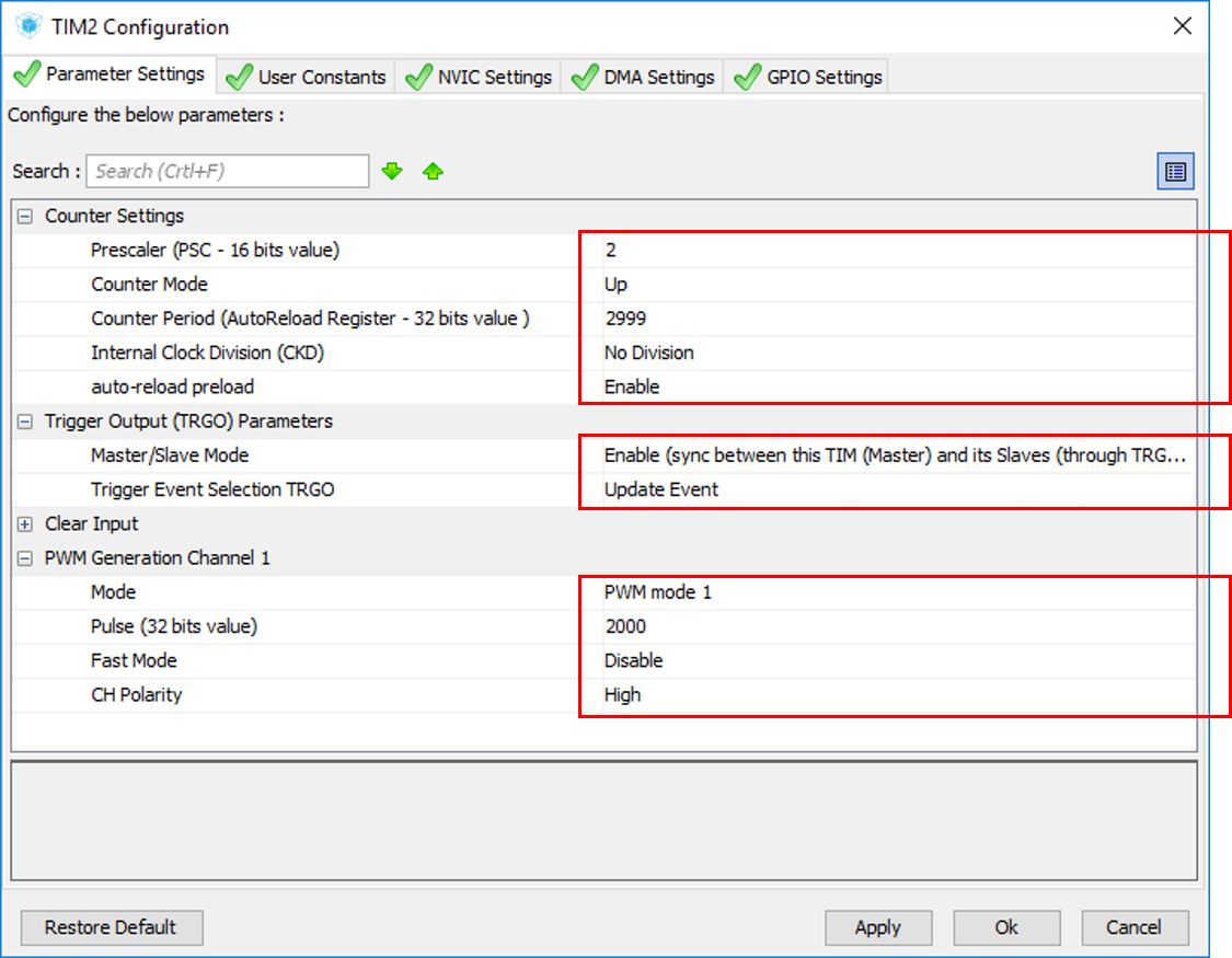 TIM2 configuration
Timer 8 for ADC Tigger
Trigger Ouput (TRGO) Parameters is where we set up trigger that will be sent to the ADC. This needs to match the ADC. Here I use TRGO2 the dedicated one and use the update event, which I later see is the wrong choice as the UEV only happens when he Repition Counter is 0, so once per cycle, so below you see I change this to Compare Pulse
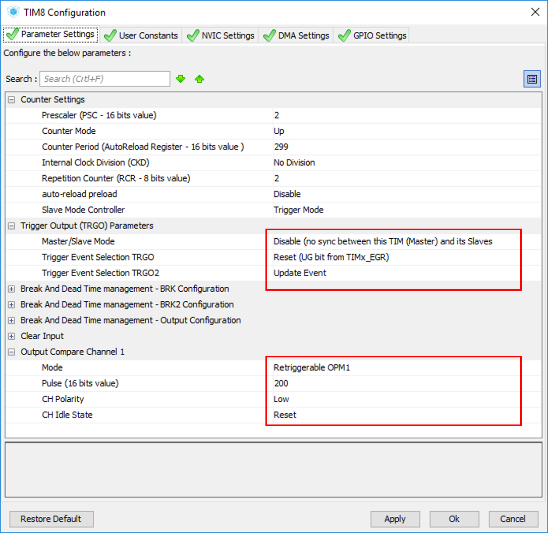 TIM8 configuration
Using PWM1 or OPM1 for TIM8 has no difference in this case, but OC mode allows more options like Toggle, of force high than I can use.
Complete the CubeMX generated code
To get it working
- Start the Timers
- Start the ADC
- Add code to handle the ADC conversion complete interupt
int main(void)
    {
    ...
    /* USER CODE BEGIN 2 */
    HAL_TIM_PWM_Start(&htim2,TIM_CHANNEL_1);
    HAL_TIM_OC_Start(&htim8,TIM_CHANNEL_1);
    HAL_ADC_Start_IT(&hadc1);
Process the data
To lessen the content I have ommitted any real processing of the data. For this guide I just toggle the User LED to inducte that the interupt is working and therefore a ADC conversion is also working.
void HAL_ADC_ConvCpltCallback(ADC_HandleTypeDef* hadc){
    HAL_GPIO_TogglePin(LD2_GPIO_Port, LD2_Pin);
}
The Output
The following image shows the generated pulses,
- The Red is TIM2.
- The Blue is TIM8
- Repition counter is set to 2 to give 3 pulses.
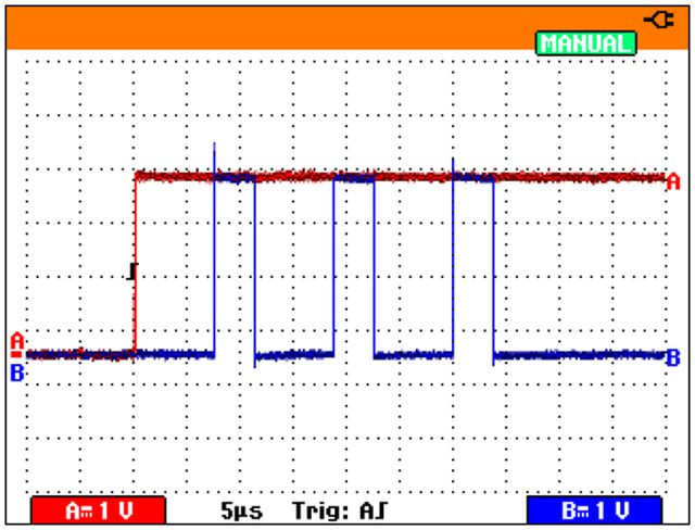 Scope attached to the TIM1_CH1 and TIM8_CH1
The following image shows TIM2_CH1 and LD2 to show the ADC conversion compelte. You can see this is not what I wanted so I need to change the TRGO2 pulse to provide a trigger every pulse.
- The Red is TIM2.
- The Blue is LD2
- Repition counter is set to 2 to give 3 pulses.
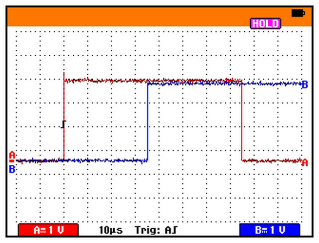 Scope attached to the TIM1_CH1 and LD2, showing conversion compelte
Success, sample where I need.
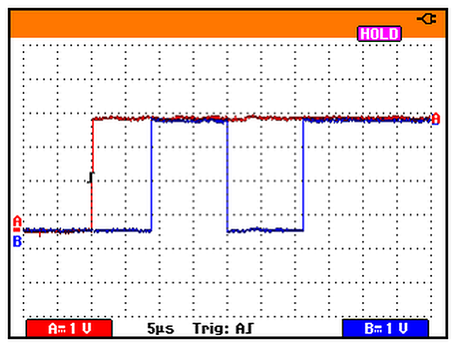 Scope attached to the Timer2 OC and LD2 (toggled on ADC EOC)
Update the timer on the fly
HAL provides three macros I use for this
- __HAL_TIME_SET_COMPARE to set the Pulse (CubeMX speak)
- __HAL_TIM_SET_AUTORELOAD to set the Counter Period
- __HAL_TIM_SET_PRESCALER to set the Prescaler
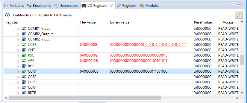 Change the timer settings for testing, direct from System Workbench.
Conclusion
The guide has stepped throguh process of creating a project to read three ADC channels using DMA and timers. These features of the low cost Nucleo boards have proven to be very powerful and convenient for a number of my projects and hope this guide will help you to realise the same.
Any questions or suggestions feel free use the contact me.
Reference
The following are the documents referenced in this guide and the key documents for any project using this STM32L476 microprocessor.
- STM32L476 reference manual, RM0351
- STM32L476je datasheet
- AN4776 Application note. General-purpose timer cookbook.